Sunday, December 6, 2009

Virtex-6 FPGAs Performance


Fall 2009 Vol. 18, No. 2

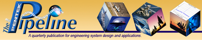
Virtex-6 FPGAs Push the Performance Envelope

With each new generation of FPGA devices, Xilinx continues to push the performance envelope to match the ever increasing requirements of target applications. The recent announcement of the Virtex-6 family is no exception. More processing power, lower power consumption and updated interface features to match the latest technology I/O requirements are all part of the new devices.

While it might be easy to assume that faster, bigger, more powerful is better, it’s important to understand how the latest FPGA innovations actually deliver this higher performance to best match the device to the specific requirements of the application.

Depending on how you interpret the Xilinx naming conventions, the Virtex-6 is the fifth or sixth generation of devices—‘Virtex-3’ was skipped over. Of these families, Virtex-4, Virtex-5 and, of course, Virtex-6 are all viable processing platforms; they are worth comparing, so that one can understand the progression of increasing performance culminating in the latest generation.

Logic Cells, Slices and CLBs

Virtex FPGAs follow a naming convention that includes the size of the device in the name. Specifically the approximate number of Logic Cells contained in the part is included in the part number. For example a Virtex-6 LX240T device contains approximately 240,000 Logic Cells, while a Virtex-5 SX95T contains approximately 95,000 Logic Cells. Sounds simple, and it is, but just comparing the amount of Logic Cells can be misleading.

Logic Cells consist of combinational logic that creates a lookup table which implements functions such as AND, OR, NAND, and addition. Flip flops and the connections to the adjacent cells are also implemented in the Logic Cell. Multiple Logic Cells are grouped together to create a single unit, called a Slice.

As the architecture of the Virtex has evolved, the number of Logic Cells in a Slice has changed: a Virtex-4 Slice consists of two Logic Cells, Virtex-5 and Virtex-6 Slices consist of six Logic Cells.

The next step up on the architectural hierarchy is the CLB (Configurable Logic Block). Here again, the development of more powerful CLBs has changed the relationship between Slices and CLBs: a Virtex-4 CLB consists of four Slices and Virtex-5 and Virtex-6 CLBs consist of two Slices. As a result, Virtex-4 CLBs require eight Logic Cells and Virtex-5 or Virtex-6 require 12 Logic Cells. Figure 1 compares these parameters in the three Xilinx generations.

So why did Xilinx design FPGA logic in this hierarchical organization instead of just creating a flat plane of interconnected Logic Cells? The multilevel design of modern FPGA devices creates a balance between interconnect speed and interconnect flexibility.

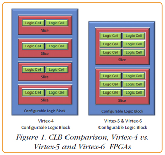
The fastest connections exist between Logic Cells. Connections between Slices are slower and connections between CLBs are even a little slower. Going in the other direction, connections between CLBs are the most flexible and general purpose, Slice connections are a bit less flexible, and connections between Logic Cells are more limited.

Increasing Density

With each new generation of FPGAs, comes higher component density in the form of more Logic Cells. Figure 2 graphs the Logic Cell densities of various devices from the last three Virtex generations. For each generation, Xilinx offers a range of different density devices within a single package type. To focus the scope of this comparison, all of the devices compared are available in the same 35 mm x 35 mm BGA (Ball-Grid Array) package.

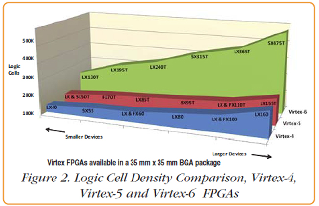
Since Virtex-4 CLBs comprise eight Logic Cells, while Virtex-5 and Virtex-6 CLBs comprise 12, the increase in Logic Cells between Virtex-4 and Virtex-5 actually translates to a decrease in CLBs because each CLB in the Virtex-5 requires more Logic Cells. While the Virtex-5 CLBs are more powerful than their Virtex-4 counterparts, there are still fewer of them to use. What is also clear from this graph is that the Virtex-6 represents a significant increase in density from the Virtex-5 family.

Geometries, Speed and Power

So how are more Logic Cells packed into the same size package with each new generation? As you might expect, by shrinking the physical size of the logic. IC geometries are measured in nm (nanometers). The progression from Virtex-4 through Virtex-6 has been from 90 nm to 65 nm to 40 nm. An additional benefit of shrinking transistors is an increase in switching rates which translates to faster clock speeds. Virtex-4 runs at 500 MHz, Virtex-5 runs at 550 MHz and Virtex-6 achieves a 600 MHz clock rate.

Unfortunately, whether it’s lunch or shrinking transistors, nothing comes for free. Leakage current tends to increase exponentially as the transistors shrink, increasing the static power, even when the transistors aren’t switching. To compensate, Xilinx has introduced a series of power saving design techniques. Depending on the mode the FPGA is operating, a power savings of between 20% and 40% can be achieved on the Virtex-6 when compared to comparable Virtex-4 devices. Again, as densities increase and more Logic Cells are packed in the same size device, these power savings become imperative.

DSPs and Memory

In addition to CLBs, Virtex FPGAs contain DSP Slices. These are dedicated multipliers, multiply-accumulator or multiply-adder blocks. The DSP slices are responsible for the majority of the processing horsepower of FPGAs. Like the CLBs, the DSPs benefit from a compound performance increase with each new generation: improvements in the actual DSP logic; increases in operational speed from 500 MHz to 550 MHz to 600 MHz with the latest generation; and increasing density allowing more DSP slices to be included in the same size package. While the largest Virtex-4 device includes 512 DSP Slices, the Virtex-6 tops out at an impressive 2016.

All Virtex FPGAs include integrated memory blocks (Block RAM) for implementing anything from random access storage to dual-port architectures, to FIFOs — depending on the application. For the 35 mm x 35 mm package we’ve been comparing, Block RAM has increased from a maximum of approximately 7 megabits to 8 megabits between the Virtex-4 and Virtex-5; it then took a sizable leap to a maximum of 38 megabits for the Virtex-6.

Connecting it all together

Through the last few generations of Virtex devices, BGA ball pitch has remained the same at 1 mm, which means there is 1 mm spacing between the BGA balls. In a 35 mm x 35 mm device, this turns out to be between 1136 and 1152 pins, depending on the device. Because of this, I/O density hasn’t really seen an increase, but the number of different I/O signal types has been expanded as well as I/O speed. The general purpose I/O, SelectIO, is used for connecting everything from devices like A/Ds and D/As, creating parallel data buses, or implementing memory interfaces. The Virtex-6 family is compatible with the latest QDRII+ and DDR3 technology and Xilinx provides examples for implementing interfaces to these devices.

A key interface feature of all of the current Virtex generations is gigabit serial transceivers. Originally named RocketIO and now GTX transceivers, these provide an essential high-speed interface for moving data on and off the FPGA. Like the SelectI/O, GTX transceivers have remained similar in number, a maximum between 16 and 20 on the 35 mm square devices we’ve been comparing. These interfaces can be used to implement different protocols, such as Serial RapidIO and Xilinx’s own Aurora, a license-free, lightweight protocol ideal for fast point-to-point data connections.

With PCI Express rapidly becoming more prevalent in systems from desktop PCs to targeted digital signal processing subsystems, Xilinx has included integrated PCI Express cores designed to support the gigabit serial transceivers. Virtex-6 supports PCI Express Base Specification 2.0 in x1 through x8 configurations.

As Figure 3 shows, each new generation of FPGAs is enabled by a range of technical advances. These span broad improvements like power reduction and device density to the intricacies of data pipelining and the addition of a single strategically placed flipflop in the CLB that an experienced FPGA engineer will exploit to the fullest. But even from just looking at the few metrics compared in this article, it’s easy to see the ongoing progression of FPGA technology and why FPGAs continue to be a preferred platform for digital signal processing.

Thursday, November 26, 2009

IP camera boasts 1080p video at 30fps

By Eric Brown


Texas Instruments (TI) announced a DaVinci-family, HD-ready Internet Protocol (IP) camera reference design. The Linux-ready DM368IPNC-MT5 is built by Appro Photoelectron, incorporates a TI DM36x-400 SoC, and can process H.264 main-profile 1080p video at 30fps while consuming only three Watts, says TI.


The DM368IPNC-MT5 is designed for cost-sensitive products requiring full HD video, such as IP cameras or IP modules for closed-circuit TV cameras, says TI. Equipped with a five megapixel Micron Aptina CMOS sensor, the DM368IPNC-MT5 IP reference design provides an Ethernet port, a RS485 serial port, a SD card, a USB interface, and Composite video output, says TI. The 2.4 x 1.8 x 3.4-inch (60 x 45 x 87mm) camera is claimed to utilize only three Watts, and includes a TI Power-over-Ethernet (PoE) "solution," called the TPS23753.


DM368 IP camera design block diagram

(Click to enlarge)

The DM368 design provides 30 percent more host processing performance than TI's previous generation IP camera reference design, offering "more headroom for differentiation and video analytics," says the company. TI appears to be comparing the DM368 design to the DM365 camera design (pictured below, right), announced in March, which was also developed in partnership with Appro.


New DM368 IP camera design (left) and earlier DM365 design (right)

The DM365 reference design is built on what TI calls a "new" DaVinci processor, the TI DM36x-400. A search for a "TMS320DM3658" DaVinci part comes up empty, but whatever the actual name of the processor, the TI DM36x-400 is likely to be a 400MHz variation of the 300Mhz TMS320DM365 SoC (system-on-chip) available with the DM365 IP camera design.

The TMS320DM365 began sampling in March, and was billed as is a higher-end version of TI's sub-$10, 720p-capable TMS320DM355, which launched in late 2007 and has been used in previous TI IP camera reference designs. Recently, TI also shipped a similar TMS320DM357SoC model that is twice as expensive as the older DM355, but which adds H.264 compression, an Ethernet MAC, and a DDR2 memory controller.

Aimed at media playback and camera-driven applications, the DM365 SoC is equipped with a 300MHz ARM926EJ-S core, plus multiple on-board peripherals. Like other DaVinci processors, it is available with a Linux-ready evaluation kit.

The SoC was touted as capable of processing 720p video at 30 frames per second (fps) or 1080p at a reduced frame rate, using the H.264 format. By comparison, the new DM36x-400 SoC and camera design boast 720p video at 60fps or 1080p at 30fps using H.264. The new design is also capable of processing 720p at 60fps using MPEG-4, or MJPEG video processed at five megapixels running at 15fps, says the company.

Like the DM365, the TI DM36x-400 offers TI's fifth-generation ISP (image signal processor), which is exploited by the new IP camera, says TI. The ISP is said to enable video stabilization, face detection, and other video quality enhancements. Other embedded functionality is said to include a web server and support for motion detection.

Linux package offers ISP tuning, encryption support

All these functions are supported by a royalty-free Linux application software package, offered with source code. The package includes an ISP Tuning Tool 1.0, a hardware-accelerated AES encryption module, and support for the Physical Security Interoperability Alliance standard (PSIA), says the company.

The software is also said to support the camera's global dynamic range enhancement (GDRE) capability. GDRE is said to enable users to "bring out details in the shadows of the video without washing out the highlights, a critical feature for video surveillance."

Availability

The DM368IPNC-MT5 IP camera reference design is available now for $995 from Appro, here, says TI. A TI page on the camera should be here.

TI will demonstrate the design at the the Global Sourcing Conference on Public Safety and Security (CPSE), on November 1-4 at the Shenzhen Convention and Exhibition Center, Futian Central District, Shenzhen, China. TI's booth may be found in Hall 1, Overseas Area A, #B218 - B223.

Thursday, November 12, 2009

United Technologies To Buy GE's Security Business for $1.82B

HARTFORD, Conn. – United Technologies Corp. (NYSE:UTX), today announced it has reached an agreement to purchase the GE Security business from GE (NYSE: GE) for $1.82 billion. The closing is pending regulatory approvals.

GE Security, part of GE Technology Infrastructure, supplies security and life safety technologies through a broad product portfolio for commercial and residential applications that include fire detection and life safety systems, intrusion alarms, and video surveillance and access control systems. Headquartered in Bradenton, Fla., the business has eight manufacturing facilities and approximately 4,700 employees in 26 countries.

"This acquisition enhances UTC Fire & Security’s status as a leading franchise in the $100 billion global fire safety and electronic security industry," UTC President and Chief Executive Officer Louis Chênevert said. "It strengthens our North America footprint, extends our capabilities and complements our existing fire and security businesses."

"The acquisition also brings additional world class product lines to the UTC portfolio, improves our aftermarket revenue potential and will deliver solid long-term value for UTC shareholders," Chênevert continued. "We expect this transaction will be earnings neutral to UTC in 2010, after restructuring and transaction costs, and anticipate that the cost synergies will make it accretive in 2011 and beyond.”

Headquartered in Connecticut, UTC Fire & Security is a business unit of United Technologies Corp., which provides high technology products and services to the building and aerospace industries worldwide. More information about UTC Fire & Security can be found at website: www.utcfireandsecurity.com.


Sunday, November 8, 2009

Lowest Cost, Lowest Power FPGAs - Cyclone IV

http://www.altera.com/b/cyclone-iv.html


SAN JOSE, Calif.--(EON: Enhanced Online News)--Expanding on the success of the Cyclone® FPGA series and extending its transceiver leadership, Altera Corporation (NASDAQ:ALTR) today announced the new Cyclone IV FPGA family. Responding to increased low-cost bandwidth needs driven by the demand for mobile video, voice, and data access, and the hunger for high-quality 3D images, the new Cyclone IV FPGA family adds support for mainstream serial protocols while offering an optimal balance of low cost, low power and a rich supply of logic, memory and DSP capabilities.

“By rivaling the cost of ASSPs and offering unmatched flexibility, Cyclone IV FPGAs are the obvious choice for next-generation designs. The innovative features of the Cyclone IV family make it easy for designers to support multiple protocols, simplify board design and create obsolescence-proof solutions that will outlast ASSPs.”

The Cyclone IV FPGA family offers two variants. Cyclone IV GX devices have up to 150K logic elements (LEs), up to 6.5-Mbits of RAM, up to 360 multipliers, and up to eight integrated 3.125-Gbps transceivers supporting mainstream protocols including Gigabit Ethernet (GbE), SDI, CPRI, V-by-One and Cyclone IV GX has hard IP for PCI Express (PCIe). With low power consumption and packages as small as 11x11 mm, these devices address cost-sensitive, small form-factor applications in the wireless, wireline, broadcast, industrial and consumer markets. Cyclone IV E devices deliver an unprecedented combination of low cost and high functionality, and lower power by up to 25 percent compared to previous generation Cyclone products for power-sensitive applications such as handheld software-defined radio.

"Cyclone IV FPGAs will expand the reach of FPGAs like never before," said Vince Hu, vice president of product and corporate marketing at Altera. "By rivaling the cost of ASSPs and offering unmatched flexibility, Cyclone IV FPGAs are the obvious choice for next-generation designs. The innovative features of the Cyclone IV family make it easy for designers to support multiple protocols, simplify board design and create obsolescence-proof solutions that will outlast ASSPs."

For the Cyclone IV GX devices, Altera focused on reducing the total system cost. By integrating transceivers, Cyclone IV GX FPGAs eliminate external component costs and reduce power consumption up to 30 percent compared to previous generation Cyclone products combined with external transceiver PHYs. This power savings also reduces costs by eliminating the need for heat-dissipation hardware. Cyclone IV GX devices require only two power supplies which significantly simplifies PCB design and reduces board space and cost. With a focus on low cost, Cyclone IV GX smallest device is the industry’s smallest FPGA with transceivers.

Pricing and Availability

Production shipments of the EP4CGX15 and EP4C115E, the first Cyclone IV GX and Cyclone IV E devices respectively, will begin in the first quarter of 2010. Budgetary pricing for the smallest devices, the EP4CE6 and the EP4CGX15, will start as low as $3 and $6 respectively for 250K unit quantities in 2010. The three smallest Cyclone IV GX devices will be supported in the Quartus® II design software version 9.1 with the remaining Cyclone IV devices supported in the Quartus II design software version 9.1 service pack 1. For additional information regarding Altera's Cyclone IV FPGAs, visit www.altera.com/pr/cycloneiv/20091102.

More news came from EEtimes:

http://www.eetimes.com/news/semi/showArticle.jhtml?articleID=221400285


Wednesday, November 4, 2009

Low cost, Low power, and High performance FPGA - Spartan-6


The Spartan®-6 family provides leading system integration capabilities with the lowest total cost for high-volume applications. The thirteen-member family delivers expanded densities ranging from 3,400 to 148,000 logic cells, with half the power consumption of previous Spartan families and faster, more comprehensive connectivity. Built on a mature 45 nm low-power copper process technology that delivers the optimal balance of cost, power, and performance, the Spartan-6 family offers a new, more efficient, dual-register 6-input look-up table (LUT) logic and a rich selection of built-in system-level blocks. These include 18 Kb (2 x 9 Kb) block RAMs, second generation DSP48A1 slices, SDRAM memory controllers, enhanced mixed-mode clock management blocks, SelectIO™ technology, power-optimized high speed serial transceiver blocks, PCI Express™ compatible Endpoint blocks, advanced system-level power management modes, autodetect configuration options, and enhanced IP security with AES and Device DNA protection. These features provide a low-cost programmable alternative to custom ASIC products with unprecedented ease-of-use. Spartan-6 FPGAs offer the best solution for highvolume logic designs, consumer-oriented DSP designs, and cost-sensitive embedded applications. Spartan-6 FPGAs are the programmable silicon foundation for Targeted Design Platforms that deliver integrated software and hardware components to enable designers to focus on innovation as soon as their development cycle begins.

Where Low Cost, Low Power Converge with High Performance

When design requirements call for low cost and low power, the new Spartan®-6 family is the answer. This silicon foundation of the Xilinx Targeted Design Platform merges industry leading process and programmable logic technology with transceiver capabilities and controllers for advanced memory support to deliver a high-performance FPGA for cost sensitive applications. Innovation in advanced power management technology and the ability to operate at a lower power 1.0V core option enable the new Spartan-6 FPGA family to achieve 65% lower power than previous Spartan families.

At the Heart of Innovation

The sixth generation in the Spartan FPGA Series enables system developers to meet demands for new features, while at the same time reducing system costs by up to half for lower-power, ”greener” products. Supporting applications such as automotive infotainment, flat-panel displays, multi-function printers, set-top boxes, home networking, and video surveillance, Spartan-6 FPGAs offer an optimal balance of low risk, low cost, low power, and high performance.

A Proven, Industry-Leading Architecture

The Spartan-6 FPGA family’s efficient, dual-register six-input LUT logic structure leverages the industry’s leading Virtex® architecture to enable cross-platform compatibility and to increase system performance. The addition of Virtex-series system-level blocks including
DSP slices, high-speed transceivers, and PCI Express® endpoint block make for greater system-level integration than ever before

The Spartan-6 family is priced at between about $3 and $54 in high volume of 10,000 units, according to Brent Pryzbus, director of product marketing, according to EETimes.


Dispersed Storage Blog

http://dev.cleversafe.org/weblog/?p=310

Trends in the advancement of storage virtualization: advanced data virtualization

Advanced data virtualization (Part 1)
After attending the recent SNW in Phoenix, and having some time to synthesize and digest, I’m convinced that the storage virtualization products on the market today are a good first step, but are going to have to evolve.

Over the next few weeks, I’ll offer several trends we foresee will occur to realize true storage virtualization. This week’s post will focus on the trend of advanced data virtualization.

Storage virtualization is creating efficiencies by inserting a layer of abstraction between data and storage hardware, and that same concept can be taken further to present a layer of abstraction between data and the method in which data is stored.

RAID is actually a well-known form of data virtualization because the linear sequence of bytes for data are transformed to stripe the data across the array, and include the necessary parity bits. RAID’s data virtualization technique was designed over 20 years ago to improve data reliability and I/O performance, and it is now in the process of failing as we transition from structured data to large quantities of unstructured data.

Dispersal, as we’ve discussed in numerous posts on this blog, is a natural successor for RAID for data virtualization because it can be configured with M of N fault tolerance, which can provide much higher levels of data reliability than RAID. Dispersal essentially packetizes the data (N packets), and only requires a subset (M packets) to bit perfectly recreate the data.

One major change for data virtualization that will occur as Dispersal replaces RAID is that there will no longer be a tight coupling between hardware and the storage of the data packets. This will eliminate the concept of having copies of data on hardware.

Today’s RAID systems stripe data and parity bits across disks within an array within an appliance. When asked “Where is my data?” the answer is typically “On this piece of hardware.” This gives people peace of mind in terms of sensing something that is intangible (since the data is actually virtualized) is actually tangible because it is contained within a physical device.

The shift for people will be from asking “Where is my data?” since it will be virtualized across multiple devices in multiple locations to “Is my data protected?” because the root of the first question is the second. Once people can get comfortable with actually giving up control of actually knowing exactly where their data resides, they will realize the benefits of data virtualization. A future post in this series will discuss how management systems will need to evolve to address Data Protection concerns.

The largest benefit to storing data packets across multiple hardware nodes is increased fault tolerance. RAID basically is structured to provide disk drive fault tolerance – as disk fails, and the other disks can reconstruct the data. Dispersal provides not only disk drive level fault tolerance, but also device drive fault tolerance, and even location fault tolerance. When an entire device fails, the data can be reconstructed from virtualized data packets on other devices, whether centrally located or across multiple sites.

We’ll discuss location fault tolerance in more detail in the next post.

Thursday, October 1, 2009

Cisco buy video-conferencing firm Tandberg for $3 billion

http://news.yahoo.com/s/nm/20091001/bs_nm/us_cisco_tandberg

LONDON/OSLO (Reuters) – Cisco (CSCO.O) has agreed to buy Norwegian videoconferencing company Tandberg (TAA.OL) for $3 billion, the latest in a series of bets taken on using video to drive demand for its core data transmission gear.

The world's dominant maker of Web routers and switches said buying Tandberg would strengthen its position in a $34 billion market for remote business collaboration tools and help it make underused videoconferencing more useful and less clumsy.

Cisco's head of European markets, Chris Dedicoat, said the move would complement Cisco's high-end videoconferencing serviceTelePresence and its previous acquisition of online meeting company WebEx, expanding the number of customers it can reach.

"Tandberg has a large number of video endpoints," he told Reuters on Thursday. He added that he considered the offer of 153.5 crowns per share in cash, an 11 percent premium to Tandberg's Wednesday closing price, as fair to both parties.

Tandberg shares, which had almost doubled in value this year, helped by takeover speculation, were up another 11.6 percent at 154.40 Norwegian crowns by 1044 GMT.

"This sounds like a pretty good price so I would think it will end up there," said analyst Martin Hoff of Arctic Securities. "But the bid will stand for four weeks and there might be other (offers)."

Potential counterbidders include Hewlett-Packard (HPQ.N), which is also active in Web collaboration. Telecoms equipment maker Ericsson (ERICb.ST) and private equity firm Silver Lake have also been linked by the market with Tandberg.

DnB NOR Markets also named in a report companies such as Juniper (JNPR.O), IBM (IBM.N), Sony (6758.T) and Siemens (SIEGn.DE) as potential suitors.

However, Tandberg's board unanimously recommended the Cisco offer to its shareholders. Cisco said it hopes to close the deal in the first half of 2010, subject to regulatory approval.

If the deal goes through Tandberg's chief executive, Fredrik Halvorsen, will continue to lead the unit.

"We have the same vision, a vision of how people communicate and collaborate," Halvorsen said on a webcast on Tandberg's website (www.tandberg.com)

"The bid makes perfect industrial sense for Cisco," said Arild Nysaether, an analyst at Fondsfinans in Oslo. "It is obvious that there are great synergies here, but it seems that Tandberg shareholders are offered none."

JP Morgan is advising Tandberg and Lazard is advising Cisco.

BET ON VIDEO

Cisco, which had $35 billion in cash as of July 25, has made decisive moves outside its core network business in recent months as large technology companies start to compete in new areas, though it has been cautious about large acquisitions.

Its largest this year was of Flip digital camcorder maker Pure Digital Technologies for $590 million in stock, expanding its presence in consumer markets and betting on the growing volume of video sent over the Internet.

In March Cisco also made its first foray into the computer server market, pitting it against longstanding partners IBM (IBM.N) and HP and hoping to exploit the ubiquity of its network equipment in data centers.

By acquiring Tandberg, Cisco reckons it can bring videoconferencing to many more companies than the thousands who currently use it, bringing its network expertise to make the experience easier.

It will also help it compete better with U.S. video conferencing products maker Polycom (PLCM.O).

"We're making video a service on the network," Dedicoat said. "It's all about interoperability," he added, referring to the current difficulty of videoconferencing, which often involves companies using technology unconnected to other systems they use.

Companies have also been stirred to try harder to make video meetings work by the recession, which has slashed corporate travel budgets and when the economy recovers companies are not expected to restore travel budgets to previous levels.

Cisco has said it has reduced its own global travel expenditure to about $260 million from $720 million, thanks to its investment in TelePresence.

Dedicoat said Cisco aimed to make remote communication a more human experience.

"We've all been on a conference call late at night where you're a voice on a speakerphone at the other end of the world, and there's 16 people in the other room," he said.

"Human beings like to meet face to face, that's how we like to communicate. However, if you can't meet face to face, and with the emphasis on carbon reduction, then you recreate as closely as you possibly can that face-to face meeting."

($1=5.794 Norwegian crowns)

(Additional reporting by Joachim Dagenborg, Tejre Solsvik and Wojciech Moskwa in Oslo; Editing by Greg Mahlich)

Friday, September 25, 2009

Matlab Simulink and HDL

Simulink HDL Coder 1.6

Generate HDL code from Simulink models and MATLAB code


You can use Simulink to model your system and then automatically generate bit-true, cycle-accurate, synthesizable Verilog and VHDL code and test benches.

Simulink® HDL Coder™ generates bit-true, cycle-accurate, synthesizable Verilog and VHDL code from Simulink® models, Stateflow® charts, and Embedded MATLAB™ code. The automatically generated HDL code is target independent.

The Simulink HDL Coder product generates Verilog code that complies with the IEEE 1364-2001 standard and VHDL code that complies with the IEEE 1076 standard. As a result, you can verify the automatically generated HDL code using popular functional verification products, including Cadence® Incisive®, Mentor Graphics® ModelSim®, and Synopsys® VCS®. You can also map the automatically generated HDL code into field-programmable gate arrays (FPGAs) or application-specific integrated circuits (ASICs) using popular synthesis tools, such as Altera® Quartus® II, Cadence Encounter® RTL Compiler, Mentor Graphics® Precision®, Synopsys Design Compiler®, Synplicity® Synplify®, and Xilinx® ISE™.

Simulink HDL Coder also generates HDL test benches that help you verify the generated HDL code using HDL simulation tools.

Charles Fulks at Intuitive Research and Technology gives example codes in

http://www.irtc-hq.com/fpga.php


Embedded Systems Conference example files
File

esc_sv09.mdl
esc_sv09_init.m
esc_sv09_pwm_pkg.m
esc_sv09_sin_pkg.m
esc_sv09_stop.m
esc_sv09_fpga.do
esc_sv09_fpga_tb.vhd
tb_utilities_pkg.vhd
esc_sv09_fpga.vhd
esc_sv09_pwm.vhd
esc_sv09_pwm_pkg.m
esc_sv09_sin.vhd
esc_sv09_sin_pkg.vhd
Description

Simulink model
Matlab script
Matlab script
Matlab script
Matlab script
ModelSim script
VHDL Testbench
VHDL Testbench package
VHDL Top Level Design
VHDL PWM Design
VHDL PWM Package (generated by Matlab script)
VHDL PWM Design
VHDL PWM Package (generated by Matlab script)


His model based FPGA design principle can be seen at

http://sedware.com/sites/default/files/FPGA_Introduction.pdf

http://sedware.com/sites/default/files/VHDL.pdf

Tuesday, September 15, 2009

Harmonic's HD Encoder

Altera's Stratix III FPGAs Chosen for Harmonic's Next-Generation Universal Broadcast Video Encoder

San Jose, Calif., April 20, 2009—Altera Corporation (NASDAQ: ALTR) today announced that Harmonic has chosen its Stratix® III FPGAs for its next-generation high-definition (HD) H.264 1080p video broadcast encoder. Delivering the right combination of performance, programmability, flexibility and low power consumption, the Stratix III devices help Harmonic to improve video quality while consuming significantly less bandwidth.

Altera® Stratix III devices are used in Harmonic's DiviCom Electra 8000, the world's first encoding and transcoding platform to support MPEG-4 AVC (H.264) and MPEG-2 CODECs in standard-definition (SD) and HD formats up to full frame-rate 1080p 50/60. While helping to provide superior picture quality, Altera's Stratix III devices also contribute to the Electra 8000&'s ground-breaking energy efficiency.

“Harmonic's DiviCom Electra 8000 sets the benchmark for real-time video-processing technology,” said Nimrod Ben-Natan, Vice President of Product Marketing, Solutions and Strategy for Harmonic Inc. “Altera's Stratix III FPGAs help us enhance our video algorithms. Altera offers clear FPGA leadership in digital signal processing (DSP) and external memory performance, while still delivering low power requirements.”

“Altera has made significant investments in our FPGA architecture and solutions to meet the demanding requirements of 1080p video-processing applications,” said Arun Iyengar, senior director of Altera's broadcast and communications business units. “Altera's Stratix III FPGAs deliver twice the video-processing capability of previous-generation FPGAs while maintaining a constant power budget. This allows broadcast leaders like Harmonic to further differentiate its products.”

Monday, September 14, 2009

H.264 Soft Encoder Comparison

H.264 Predefined profiles

H.264 Profile Level

IBC 2009: Tandberg Unveils HD H.264

http://webcast.broadcastnewsroom.com/articles/viewarticle.jsp?id=842482&afterinter=true

IBC 2009: Tandberg Unveils Next-Generation MPEG-4 Gear

Shows complete contribution system

By Glen Dickson

IBC Amsterdam 2009: Complete Coverage of the IBC Show


Ericsson unit Tandberg Television introduced at IBC new MPEG-4 encoding products aimed at both backhauling high-definition signals and distributing them directly to consumers.


According to Tandberg VP of technology Matthew Goldman, Tandberg is the only vendor to provide a complete MPEG-4 AVC HD 4:2:2 system solution for the C&D (Contribution and Distribution) market, i.e. either backhauling signals from live events or distributing high-quality mezzanine feeds to cable headends which will then be re-compressed for delivery to the home. It was demonstrating the system in its joint Tandberg/Ericsson booth.


The new MPEG-4 4:2:2 system, which uses 10-bit video processing for improved color gradation, supports HD encoding up to the 1080p/60 format. It includes the existing Tandberg RX8200 receiver, which can be upgraded to support 4:2:2 10-bit encoding through a software option. Goldman expects the 4:2:2 system will eventually be used to backhaul feeds produced in the 1080p/60 format at bit-rates ranging from 20 to 80 Mbps.


"That's in the sweet spot that JPEG2000 can't hit," says Goldman.


Tandberg also introduced the EN8190 HD encoder, an MPEG-4 4:2:0 product aimed at direct-to-home (DTH) satellite applications as well as the IPTV market. Goldman says the EN8190 represents a 20-25% improvement in bit-rate efficiency over the company's previous MPEG-4 4:2:0 model, enough for a DTH operator to add one more HD channel per satellite transponder. Tandberg was demonstrating the EN8190 delivering six HD channels in 30 Mbps of bandwidth using its statistical multiplexing technology.


In another part of its booth, Tandberg was explaining how its OpenStream VOD management system can be used today to support multi-platform delivery. The demonstration showed how a VOD movie that was being delivered to a basic Motorola DCT-2000 set-top box could be paused, with the movie then being restarted as streaming video delivered to an Apple iPhone over a Wi-Fi link.


Tandberg VP of applications software strategy Michael Adams says the company will give a more in-depth demonstration of OpenStream's multiplatform capabilities at the SCTE show in Denver next month. He says the streaming form of VOD could be delivered just as easily over a wireless 3G network as over a Wi-Fi link.


"That's just a plumbing issue," says Adams, who expects that Tandberg will be involved in a commercial deployment of such multi-platform delivery by early next year.


Broadcasting & Cable Copyright © 2008 Reed Business Information A division of Reed Elsevier Inc. All rights reserved.

Tuesday, September 8, 2009

Verilog Primer

  • Chapter1: Introduction to Verilog hardware description language
  • Chapter 2: Verilog Structure
    • 2.1 Modules
    • 2.2 Structural Design with Gate Primitives and the Delay operator
    • 2.3 Structural Design with Assignment Statements
    • 2.4 Structural Design with using Modules
    • 2.5 Behavioral Design with Initial and Always blocks
  • Chapter 3: Verilog Syntax Details
    • 3.1 Structural Data Types: wire and reg
    • 3.2 Behavioral Data Types: integer, real, and time
    • 3.3 Number Syntax
    • 3.4 Behavioral Design with blocking and non-blocking statements
    • 3.5 Arrays, Vectors, and Memories
    • 3.6 Operators
  • Chapter 4: Verilog Design Flow
    • Step 1: Create RTL Design Models and Behavioral Test Bench Code
    • Step 2: Functionally Simulate your Register-Transfer-Level Design
    • Step 3: Convert RTL-level files to a Gate-level model with a Synthesizer
    • Step 4: Perform Gate Level simulations with FPGA or ASIC libraries
    • Optional Step: Gate-level simulation with SDF timing information
Info site for timing diagrams

Saturday, September 5, 2009

Aptina 1080p CMOS Sensor

It is called MT9J001. The detail info need to be viewed under NDA. The following is their press release.

http://www.micron.com/about/news/pressrelease.aspx?id=99025FDDEFA2B68E

San Jose, CA and Cologne, Germany , Tuesday, September 23, 2008 – Continuing to push the capabilities of high performance CMOS image sensors, Aptina Imaging, today introduced its new 10-megapixel (part number MT9J001) sensor for digital still camera, digital video and hybrid camera applications. The sensor provides camera manufacturers with an easy to integrate, unique sensor that combines rapid image capture and superior image quality. The new 1.67-micron pixel sensor features 1/2.3” optical format, and a parallel/serial frame rate of 7.5fps (parallel) and 15fps (serial). It is the first 10MP CMOS image sensor for point-and-shoot digital cameras and the first product to integrate Aptina’s High-Speed Serial Pixel Interface (HiSPi™). This high bandwidth serial interface is based upon the JEDEC SLVS signaling standard and enables faster data transfer rates (up to 2.8 Gbps). Aptina’s new sensor features HiSPi™ and allows a camera to capture and process data in HD (1080p/60fps). Additionally, the new 10MP sensor is the first of Aptina’s high performance sensors with digital re-sampling after binning. This re-sampling feature removes binning artifacts seen in 2x2 binned images and matches the distribution density of the original unbinned image. As a result of the extended binning capabilities of the sensor, camera users have a full field of view in HD, enhancing the overall end-user experience. Aptina’s announcement comes as the Photokina 2008 international tradeshow in Cologne, Germany begins.

"Aptina CMOS technology is advancing rapidly, enabling us to create high performance camera products for our global customers," says Sandor Barna, Vice President of Marketing at Aptina. "Our new 10MP image sensor incorporates a unique 1.67-micron pixel format and a four-lane HiSPi™ serial data interface to achieve results unmatched by CCD technology such as 60 fps HD video capture at 1080p."

HiSPi™ is the High Speed Serial Pixel Interface developed and owned by Aptina Imaging. The open access, scalable technology enables 1080p/60 fps performance (and beyond) and has been adopted by many of Aptina’s business partners to meet the challenges of high speed, low power consumption data transfer. HiSPi™ technology provides distinct benefits for users including open access to a performance focused interface, the ability to support 1080p/60fps today—4X the data rate of standard broadcast (DI)—and the scalability to accommodate higher data rates for the future. The MT9J001 10MP image sensor extends Aptina’s portfolio of higher resolution products, providing increased image quality and HD video capture like the 5MP (MT9P001), 8MP (MT9E001), and 9MP (MT9N001). Samples will be available in 4Q08 and limited production begins in 1Q09.

Omnivision 1080p CMOS Sensor


The OV2710 is a true full HD (1080p) CMOS image sensor designed specifically to deliver high-end HD video to digital video camcorders, notebooks, netbooks, PC webcamand other mobile applications. The 1/3-inch OV2710 addresses the fast growing demand for affordable, HD-quality digital video solutions for video conferencing and recording.


The OV2710 is among the very first no-compromise full HD (1080p) sensors available on the market, meaning it offers the HD video format with a display resolution of 1920 x 1080 pixels, operating at 30 frames per second. Built with OmniVision's proprietary 3 μm OmniPixel3-HS™ high sensitivity pixel technology, the OV2710 delivers low-light sensitivity of 3300 mV/lux-sec, dark current of 6 mV/sec and a peak dynamic range of 69 dB. This enables cameras to operate in virtually every lighting condition from bright daylight to nearly complete darkness below 15 lux.


The OV2710 supports multiple platform architectures and controllers with both parallel and MIPI interfaces. By allowing system designers to leverage the same opto-electrical design across various products and multiple market segments, the OV2710 significantly reduces product development time. OmniVision's OmniPixel3-HS pixel technology has already been proven in high quality webcam/video applications and is now available in 1080p full HD in the OV2710.


Followers

Blog Archive

About Me

My photo
HD Multimedia Technology player