 | |||
Fall 2009 Vol. 18, No. 2 | |||
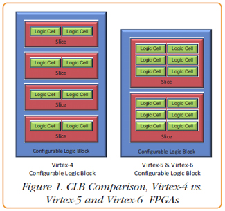
Virtex-6 FPGAs Push the Performance EnvelopeWith each new generation of FPGA devices, Xilinx continues to push the performance envelope to match the ever increasing requirements of target applications. The recent announcement of the Virtex-6 family is no exception. More processing power, lower power consumption and updated interface features to match the latest technology I/O requirements are all part of the new devices. While it might be easy to assume that faster, bigger, more powerful is better, it’s important to understand how the latest FPGA innovations actually deliver this higher performance to best match the device to the specific requirements of the application. Depending on how you interpret the Xilinx naming conventions, the Virtex-6 is the fifth or sixth generation of devices—‘Virtex-3’ was skipped over. Of these families, Virtex-4, Virtex-5 and, of course, Virtex-6 are all viable processing platforms; they are worth comparing, so that one can understand the progression of increasing performance culminating in the latest generation. Logic Cells, Slices and CLBsVirtex FPGAs follow a naming convention that includes the size of the device in the name. Specifically the approximate number of Logic Cells contained in the part is included in the part number. For example a Virtex-6 LX240T device contains approximately 240,000 Logic Cells, while a Virtex-5 SX95T contains approximately 95,000 Logic Cells. Sounds simple, and it is, but just comparing the amount of Logic Cells can be misleading. Logic Cells consist of combinational logic that creates a lookup table which implements functions such as AND, OR, NAND, and addition. Flip flops and the connections to the adjacent cells are also implemented in the Logic Cell. Multiple Logic Cells are grouped together to create a single unit, called a Slice.
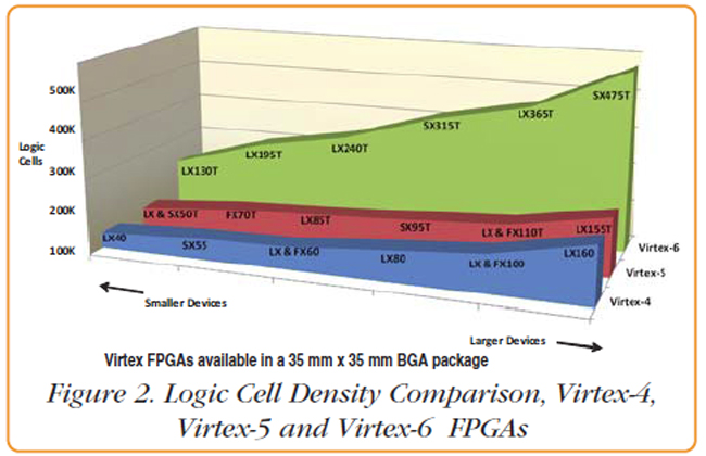
The fastest connections exist between Logic Cells. Connections between Slices are slower and connections between CLBs are even a little slower. Going in the other direction, connections between CLBs are the most flexible and general purpose, Slice connections are a bit less flexible, and connections between Logic Cells are more limited. Increasing DensityWith each new generation of FPGAs, comes higher component density in the form of more Logic Cells. Figure 2 graphs the Logic Cell densities of various devices from the last three Virtex generations. For each generation, Xilinx offers a range of different density devices within a single package type. To focus the scope of this comparison, all of the devices compared are available in the same 35 mm x 35 mm BGA (Ball-Grid Array) package.
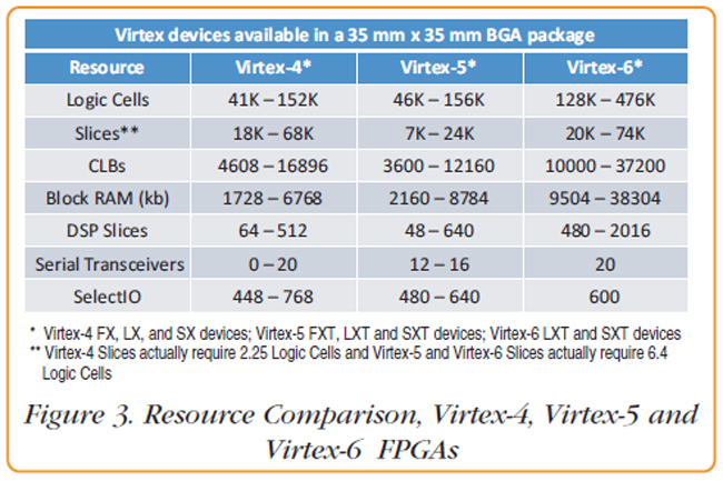
Since Virtex-4 CLBs comprise eight Logic Cells, while Virtex-5 and Virtex-6 CLBs comprise 12, the increase in Logic Cells between Virtex-4 and Virtex-5 actually translates to a decrease in CLBs because each CLB in the Virtex-5 requires more Logic Cells. While the Virtex-5 CLBs are more powerful than their Virtex-4 counterparts, there are still fewer of them to use. What is also clear from this graph is that the Virtex-6 represents a significant increase in density from the Virtex-5 family. Geometries, Speed and PowerSo how are more Logic Cells packed into the same size package with each new generation? As you might expect, by shrinking the physical size of the logic. IC geometries are measured in nm (nanometers). The progression from Virtex-4 through Virtex-6 has been from 90 nm to 65 nm to 40 nm. An additional benefit of shrinking transistors is an increase in switching rates which translates to faster clock speeds. Virtex-4 runs at 500 MHz, Virtex-5 runs at 550 MHz and Virtex-6 achieves a 600 MHz clock rate. Unfortunately, whether it’s lunch or shrinking transistors, nothing comes for free. Leakage current tends to increase exponentially as the transistors shrink, increasing the static power, even when the transistors aren’t switching. To compensate, Xilinx has introduced a series of power saving design techniques. Depending on the mode the FPGA is operating, a power savings of between 20% and 40% can be achieved on the Virtex-6 when compared to comparable Virtex-4 devices. Again, as densities increase and more Logic Cells are packed in the same size device, these power savings become imperative. DSPs and MemoryIn addition to CLBs, Virtex FPGAs contain DSP Slices. These are dedicated multipliers, multiply-accumulator or multiply-adder blocks. The DSP slices are responsible for the majority of the processing horsepower of FPGAs. Like the CLBs, the DSPs benefit from a compound performance increase with each new generation: improvements in the actual DSP logic; increases in operational speed from 500 MHz to 550 MHz to 600 MHz with the latest generation; and increasing density allowing more DSP slices to be included in the same size package. While the largest Virtex-4 device includes 512 DSP Slices, the Virtex-6 tops out at an impressive 2016. All Virtex FPGAs include integrated memory blocks (Block RAM) for implementing anything from random access storage to dual-port architectures, to FIFOs — depending on the application. For the 35 mm x 35 mm package we’ve been comparing, Block RAM has increased from a maximum of approximately 7 megabits to 8 megabits between the Virtex-4 and Virtex-5; it then took a sizable leap to a maximum of 38 megabits for the Virtex-6. Connecting it all togetherThrough the last few generations of Virtex devices, BGA ball pitch has remained the same at 1 mm, which means there is 1 mm spacing between the BGA balls. In a 35 mm x 35 mm device, this turns out to be between 1136 and 1152 pins, depending on the device. Because of this, I/O density hasn’t really seen an increase, but the number of different I/O signal types has been expanded as well as I/O speed. The general purpose I/O, SelectIO, is used for connecting everything from devices like A/Ds and D/As, creating parallel data buses, or implementing memory interfaces. The Virtex-6 family is compatible with the latest QDRII+ and DDR3 technology and Xilinx provides examples for implementing interfaces to these devices. A key interface feature of all of the current Virtex generations is gigabit serial transceivers. Originally named RocketIO and now GTX transceivers, these provide an essential high-speed interface for moving data on and off the FPGA. Like the SelectI/O, GTX transceivers have remained similar in number, a maximum between 16 and 20 on the 35 mm square devices we’ve been comparing. These interfaces can be used to implement different protocols, such as Serial RapidIO and Xilinx’s own Aurora, a license-free, lightweight protocol ideal for fast point-to-point data connections. With PCI Express rapidly becoming more prevalent in systems from desktop PCs to targeted digital signal processing subsystems, Xilinx has included integrated PCI Express cores designed to support the gigabit serial transceivers. Virtex-6 supports PCI Express Base Specification 2.0 in x1 through x8 configurations.
As Figure 3 shows, each new generation of FPGAs is enabled by a range of technical advances. These span broad improvements like power reduction and device density to the intricacies of data pipelining and the addition of a single strategically placed flipflop in the CLB that an experienced FPGA engineer will exploit to the fullest. But even from just looking at the few metrics compared in this article, it’s easy to see the ongoing progression of FPGA technology and why FPGAs continue to be a preferred platform for digital signal processing. |
Sunday, December 6, 2009
Virtex-6 FPGAs Performance
Subscribe to:
Comments (Atom)


